

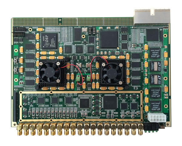
System specifications
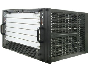
The system adopts a 6U standard CPCI architecture, which includes the following parts:
1.2 Channel 8-bit 1.5GSPS acquisition module.
2.10 Channel 14bit 125MSPS ADC module.
3.8 Channel 14bit 10MSPS ADC module.
4.2 Channel 14bit 1GSPS DAC module.
5.10 Channel 14bit 125MSPS DAC module.
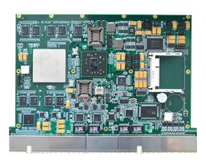
6. FPGA adopts 2 high-performance FPGAs.
7. Deploy 2GB 64 bit wide DDR3 memory per FPGA, with a total of 4GB onboard memory.
8. Expand TI 320C6455 DSP with independent DDR2 external memory and flash chip.
9. Adopting PLX9056 interface chip, supporting 66MHz 32-bit PCI bus.
10.6 485 interfaces with controllable IO direction.
11. Standard 6U CPCI board, 3-slot width.
System Block Diagram
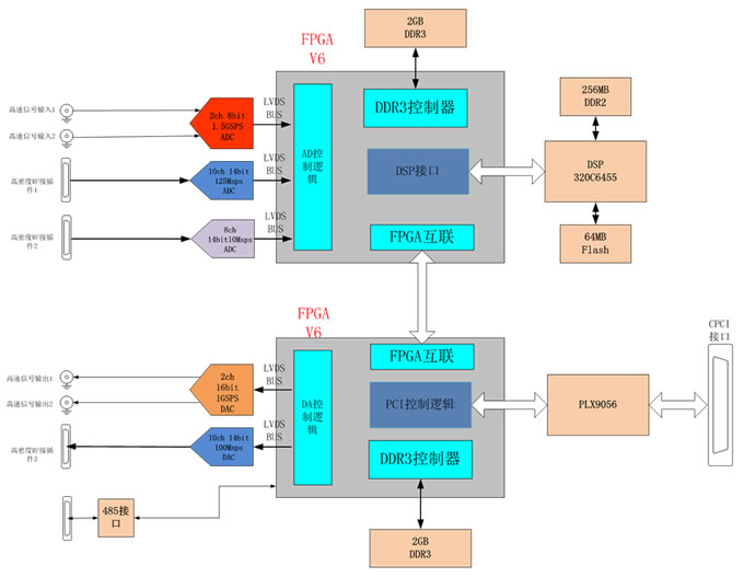
Collection module
2-channel high-speed acquisition. SMA input, single ended 50 ohms, AC coupling, input amplitude 2Vpp, 1000MHz bandwidth. The signal is input through the SMA interface and transformed into a differential signal through transformer coupling; Filters can be configured as either direct, low-pass, or bandpass, 5th order Bessel or Butterworth. All output data and accompanying clock of ADC are connected to FPGA. The acquisition clock is generated by a high-performance clock generator, and the acquisition frequency can be programmed in the range of 10MHz to 1500MHz.
The high-speed acquisition chip adopts TI's ADC08D1520 chip, which supports dual channel 1.5GSPS sampling.
ADC performance indicators: sampling frequency of 1.5GHz, Fin frequency of 373MHz, amplitude Vin=FSR -0.5dB.
3. The 10 channel acquisition adopts 14bit 125Msps, while the 8 channel acquisition adopts 14bit 10Msps, both of which are DC coupled, with a 50 ohm input impedance and high-density connectors.
The 14bit 125Msps ADC uses Linear's LTM9012 chip. This chip integrates a 4-channel 14bit 125Msps ADC.
The 8-channel acquisition adopts linear company's LTM9006 chip. A single module integrates 8 channels of 14bit 25Msps ADC, and this system operates at a sampling rate of 10Msps.
4. 2-channel high-speed DAC. SMA output, single ended 50 ohms, AC coupling, output amplitude 1Vpp, 1000MHz bandwidth.
The high-speed DAC adopts TI's DAC5681 chip, with a 16bit 1Gsps sampling rate.
5. The 10 channel DAC adopts 14bit 100Msps, all of which are DC coupled, with a 50 ohm output impedance and high-density connectors.
This DAC uses TI's DAC290414bit 125Msps chip.
6. DSP and FPGA are connected via EMIF bus.
The DSP chip is TI's TMS320C6455, which has the following performance:
The working frequency is 1.2GHz.
Computing power 9600MIPS.
32bit bit wide 256MB DDR2 memory, data frequency 533MHz.
64MB Program FLASH.
Connected to FPGA via high-speed synchronous EMIF bus.
7. FPGA module: Two high-performance FPGAs are used in parallel, and the ADC channel and DAC channel are controlled by separate FPGAs, Each FPGA has a separate DDR3 storage unit, an external 64bit DDR3 chip with a 2GB bit width, a data frequency of 1066MHz, and provides a data read and write bandwidth of 64Gbps.
96 pairs of high-speed LVDS are used for interconnection between FPGAs. Each FPGA has an independent configuration FLASH.
8. Analog input/output:
Both analog inputs and outputs use SMA interfaces, occupying a total of 3 6U slots:
Slot 1: High speed ADDA, 4 SMA; 485 interface.
Slot 2: 18 SMA, medium and low speed ADC interfaces.
Slot 3: 10 SMA, medium speed DAC interfaces.
The low-speed and medium speed analog interfaces are connected using internal high-density connectors and RF cables.
Application:
Algorithm simulation and verification, no soft radio, etc.